Designed and implemented multiple FPGA-based digital system modules, including search acceleration, VGA graphics display, and audio processing.
SystemVerilogQuartusModelSimDE1-SoC
Background / Motivation
Course and lab projects explored how digital logic becomes reliable hardware behavior on an FPGA board.
Problem Definition
Build hardware modules that combine state-machine control, datapaths, memory interfaces, graphics output, and audio processing under real timing constraints.
Technical Approach
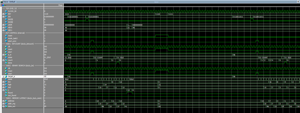
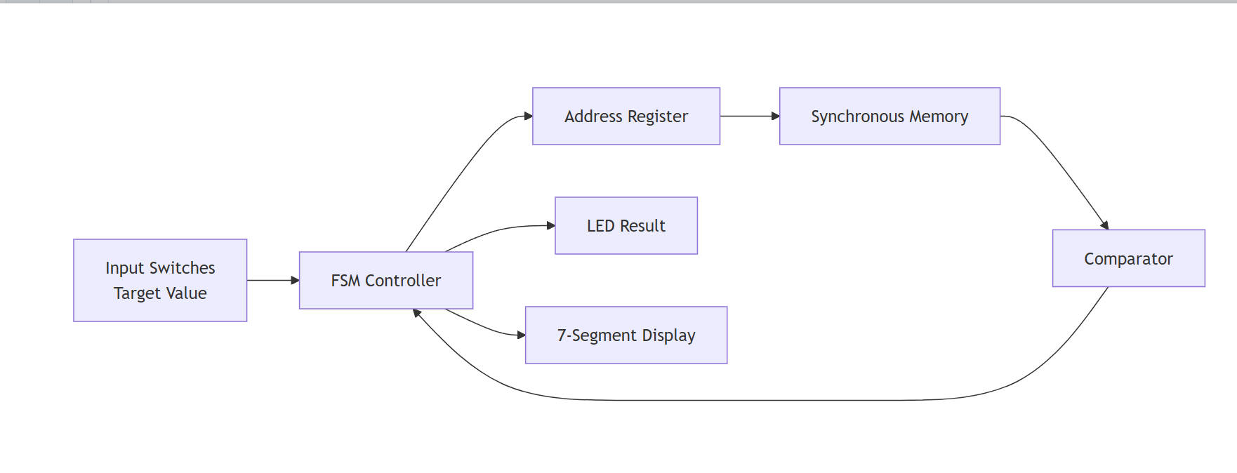
Separated each design into control and datapath blocks, validated behavior in simulation, and iterated on board-level debugging with waveform traces.
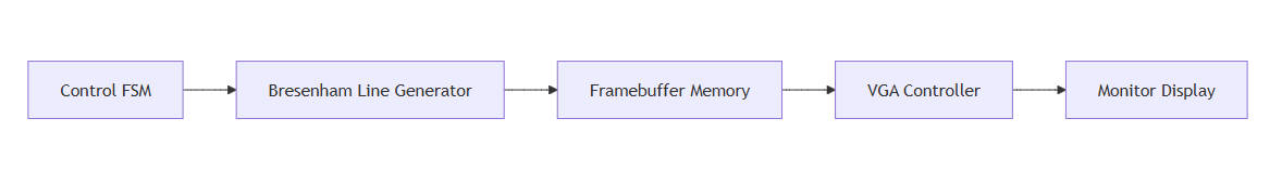
System Architecture / Design
FSM controllers coordinate datapath registers, memory reads, VGA timing logic, and audio signal modules.
Implementation Details
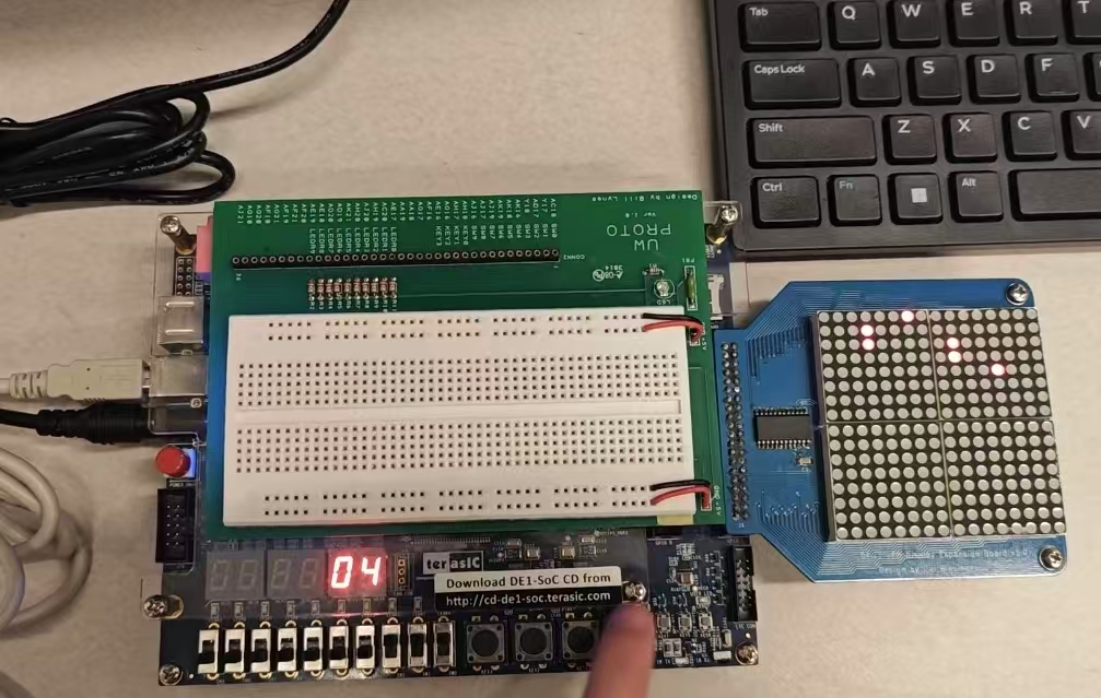
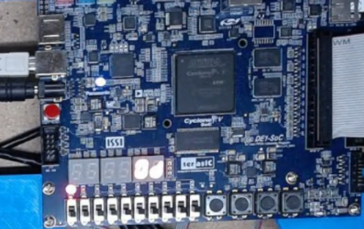
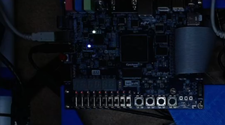
Implemented modules in SystemVerilog, simulated with ModelSim, synthesized in Quartus, and tested on DE1-SoC hardware.
Challenges and Solutions
Timing-sensitive visual output
State transition debugging
Hardware/software mismatch between simulation and board behavior
Results / Outcome
Built working FPGA modules for graphics and signal tasks
Improved waveform-based debugging workflow
Gained stronger intuition for digital hardware design
Reflection
The project strengthened my ability to reason from specification to timing-aware implementation.